Daughter Boards
The first big noticeable difference between the original PCB and the new one is the presence of a daughter board. The idea behind this is to have a main PCB that can be used for different purposes. For example, you could design a daughter board with a ZigBee module, or a daughter board with a speaker, or a daughter board with a sensor. The possibilities are endless.
The main PCB has 6 GPIOs that can be used to communicate with the daughter board. The daughter board can be powered by the main PCB... Both +5V and +3.3V are available on the daughter board.
Daughter/mother connection can be done via the BC075-10-A-L-A connector (if soldered) or wires could be hand-soldered to the 1mm pitch pads on the main PCB.
For example, you could design a daughter board with a ZigBee module, or a daughter board with a speaker, or a daughter board with a sensor. The possibilities are endless.
The main PCB has 6 GPIOs that can be used to communicate with the daughter board.
Connector
Daughter/mother connection can be done via the BC075-10-A-L-A connector (if soldered) or wires could be hand-soldered to the 1mm pitch pads on the main PCB.
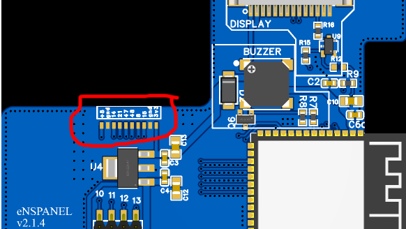
From left to right here the 10 pins:
- +5V
- GND
- IO14
- IO21
- IO47
- IO48
- IO8
- IO16
- GND
- 3.3V
Designing a Daughter Board
The daughter board can be designed in any way you like. But there are dimension constraints.
Constraints:
- max 34.6x51.4mm
- max 1.6mm thickness
- 1mm pitch for the connector
- at least 16.51 mm clearance from first connector pad to the edge of the board
- at least 8.5 mm clearance from the last connector pad to the edge of the board
All measurements are shown below:
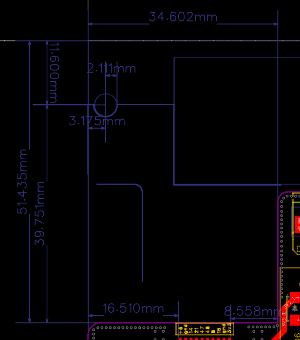
NOTE: Please mind the hole in the daughter board. The hole is there to allow the daughter board to be slotted in the enclosure. The hole is 2.1mm in radius and is centered at ~3.2mm from left edge and 11.6mm from the top edge.
NOTE: Having some clearance is always a good idea.
Also, in case you need to slot an antenna, please use the leftmost edge of the daughter board!